The global battle for 1.8-nanometer advanced manufacturing processes has intensified
The battle among global semiconductor giants for advanced manufacturing processes is becoming increasingly fierce.
Recently, Chen Liwu, the new CEO of Intel, announced that the Intel 18A process has entered the risk production stage and is planned to achieve mass production within this year. Chen Liwu emphasized that 18A is a key juncture for Intel to regain its leading position in process technology. The technical team will continue to optimize PDK and manufacturing process capabilities to ensure that mass production deliveries match customer demands. And its target rivals are precisely the two giants in the current semiconductor foundry industry - TSMC and Samsung.
The so-called 18A, or 18 anemometers (corresponding to 1.8 nanometers), is a planned process proposed by Intel since it launched the "Five Process Nodes in Four Years" plan in 2021, aiming to reverse the performance of its foundry business and regain its leading position in process technology. Its official benchmark is the 2 nanometers of TSMC and Samsung. Previously, both TSMC and Samsung announced that they would officially start production of 2-nanometer processes in 2025.
In addition to 18A, Intel also planned in its previous roadmap to further consolidate its leading position through the 14A (1.4-nanometer) node in the future. According to public information, Intel's 14A process will adopt high numerical aperture EUV lithography technology, further enhancing the performance-to-power ratio by 15% to 20%.
All signs indicate that 2025 is destined to be a crucial year that determines the global market landscape of advanced semiconductor manufacturing processes. Luo Guozhao, director of CHIP's China laboratory, told China Business Journal that for Intel, the mass production of the 18A node is an important move in its "five process nodes in four years" strategy, and it will also bring the global foundry competition into the most intense stage, with yield, delivery cycle and customer strategy becoming key variables.
The styles of the three giants are differentiated
Although the target manufacturing processes are the same, a closer look at the technical paths and promotion styles of the three giants reveals significant differences.
According to the official information released by Intel, its 18A process adopts RibbonFET gate-all-around transistors and PowerVia backside power supply technology to enhance performance and energy efficiency, especially optimized for AI and high-performance computing scenarios. In the industry's view, this means that Intel is betting more on architectural innovation. The 18A process moves the power network from the front to the back of the chip through PowerVia technology, increasing transistor density while reducing power consumption, making it the first process node in the industry to commercialize backside power supply.
In Luo Guozhao's view, this slightly radical technological route represents Intel's urgency to regain its dominance in manufacturing processes. However, Intel has experienced delays and capacity constraints at the 20A node over the past three years. Whether it can increase production on schedule remains to be tested by the market. In addition, the news of its losses in the second quarter and the delay in factory construction has also raised doubts in the market about the long-term competitiveness of its contract manufacturing business.
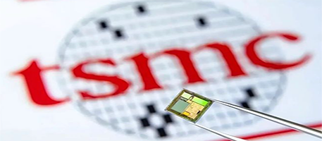
In contrast, TSMC adheres to the traditional process optimization route and simultaneously enhances the computing performance by 40 times through the SoW-X wafer-level packaging solution. In terms of advancement, TSMC's style has always been known for its "stability". Its 2-nanometer process is scheduled for mass production in the second half of 2025, while the 1.4-nanometer process is set for 2028.
And customer stickiness is the core barrier of TSMC. As of now, leading enterprises such as Apple and NVIDIA have clearly prioritized the allocation of 1.8-nanometer orders to TSMC. It is expected that in 2026, the iPhone 18 series will be the first to launch its 1.8-nanometer process chips. This positive cycle also enabled TSMC to continue leading the industry with a foundry revenue of 4.7 billion US dollars in the first quarter of 2025, representing a year-on-year growth of 7%.
Samsung lies between the two. At the foundry forum held in 2023, Samsung unveiled the roadmap for the 2GAP process, planning to mass-produce the 2-nanometer process in 2025 and commercialize the 1.4-nanometer process in 2027.
However, Luo Guozhao pointed out that although Samsung was the first to adopt GAA (Full Gate Transistor Technology) transistors at the 3-nanometer node, its frequent yield issues led to the loss of customers. This has also led to the current delay of Samsung's 2-nanometer process mass production plan to 2025. To make up for its technological shortcomings, Samsung is accelerating its layout of advanced packaging and memory chip collaboration, attempting to catch up with TSMC through a "heterogeneous integration" strategy.
The market pattern of contract manufacturing may change
With Intel's entry, the global foundry market landscape is also quietly changing.
In the semiconductor market, the essence of competition in advanced processes often stems from the scramble for customer resources. Based on various information, currently, Intel's foundry business at the 18A node has attracted 43 potential customers to test chips, including 7 of the world's top 10 chip design companies. Pat Gelsinger, the former CEO of Intel, also disclosed at an internal meeting that 18A has made a large advance payment commitment.
As a result, with the announcement of the 18A trial production, Intel's stock price has also risen as expected recently, increasing by nearly 30% in a single week and achieving its best performance since 1987.
In contrast, TSMC still holds a 66% share of the advanced process foundry market, thanks to its mature process ecosystem and the locking in of leading customers like Apple. However, its 2-nanometer node faces direct competition from Intel's 18A, especially since TSMC's 2-nanometer process does not integrate backside power supply, while Intel's 18A has a 4% performance advantage at the same power consumption.
Samsung is attempting to break the deadlock through pricing strategies and penetration into emerging markets. Its 2-nanometer process quotation is 15% to 20% lower than that of TSMC, and it has targeted customers such as Qualcomm and Japan's PFN. However, yield issues and technical reliability remain its greatest uncertainties. Journalists have noticed that Qualcomm once attempted to produce Snapdragon chips using Samsung's 4-nanometer process, but due to poor energy efficiency performance, it turned to TSMC. To make up for its shortcomings, Samsung is accelerating its cooperation with ARM and Synopsys, optimizing GAA design tools to shorten the development cycle for its customers.
Luo Guozhao believes that in the short term, GAA transistors and backside power supply will become standard equipment for 2-nanometer and even more advanced processes. Meanwhile, consumer electronics and AI chips are dominating the demand for advanced processes. Against this backdrop, if Samsung fails to solve the yield issue, it may completely exit the first echelon.
Industry analysis firm Gartner predicts that the global market size of 1.8nm and more advanced process chips will exceed 30 billion US dollars by 2028, with AI chips and high-performance computing accounting for more than 60%. However, competition in this market will not be limited to technical parameters. Supply chain resilience, cost control and the ability to build an ecosystem will become the decisive factors. Among them, if Intel can fulfill its 18A mass production commitment and attract leading customers, it is expected to rewrite the foundry market landscape after 2025. TSMC needs to accelerate the iteration of packaging technology while maintaining its process advantages. Samsung, on the other hand, needs to address the yield issue and enhance technological differentiation.


